Katharine B. Gebbie Young Investigator Award
The Sigma Xi Katharine B. Gebbie Young Investigator Award honors early-career researchers at NIST. These researchers are invited to give seminars on their work as part of the recognition. Abstracts are included below, where available.
Awardees include:
2025
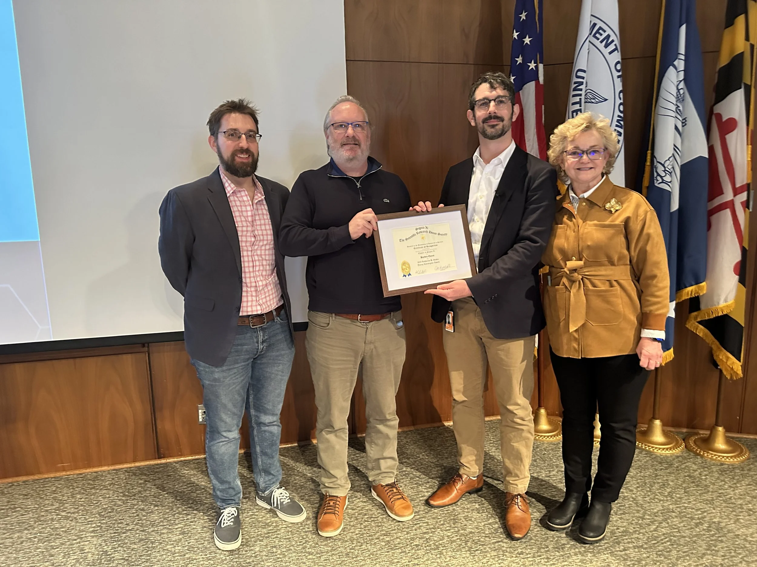
Dr. Hayden Evans, nist Center for neutron research
How Structural Dynamics in Porous Materials can Drive Next-Generation Industrial Gas Separations
Chemical separations account for nearly 15 % of energy use in the United States. Within that, small molecule gas separations, like separating oxygen from nitrogen, or hydrocarbons from contaminants, are vital to our economy, but energy and monetarily expensive. In this talk, I will explain how porous materials with extremely small (sub-nanometer) and dynamic pore windows are a potential pathway towards more efficient separation processes. To illustrate this, I will discuss my recent work on a new and industrially relevant adsorbent, aluminum formate. This material is seemingly simple, but only through careful experimental and computational analysis involving expertise across NIST could we uncover the extent and origins of its remarkable separation performance.
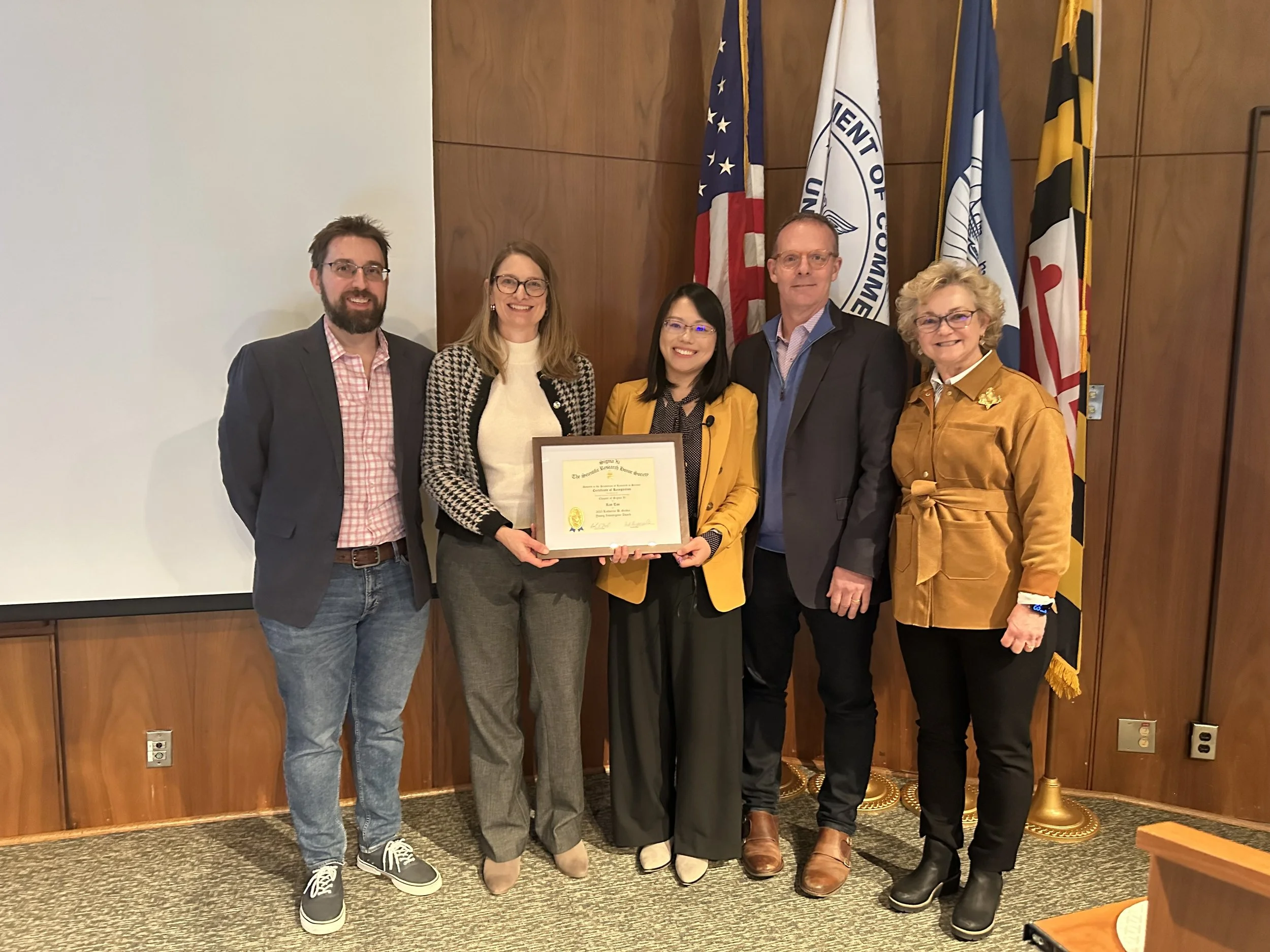
Dr. Ran Tao, Materials Measurement Science Division, Mml, nist
Quantifying Flow and Cure for Mission-Driven Research: From Body Armor to Microchips
Dr. Katharine Gebbie’s legacy at NIST reflects a simple truth: measurements unlock innovation when they are trusted, transferable, and connected to stakeholders. Modern standards and manufacturing require metrology for complex materials whose properties evolve with processing, temperature, and history. In this talk, I will describe rheology- and thermal-analysis-based methods that translate fundamental measurements into industrially relevant metrics and standards impact. Examples include validating candidate standard ballistic witness materials for body armor testing; correcting major errors in orthogonal superposition rheometry; qualifying ceramic feedstocks to advance ceramic additive manufacturing (AM) and future reference materials, and calorimetric cure kinetics measurements and modeling for epoxy systems in advanced semiconductor packaging.
2024
Dr. Nicole Yunger Halpern, Quantum Measurement division, pml, nist
Beyond the First Law: Peculiarly Quantum Conservation in Thermodynamics
The ideal quantum computer evolves in isolation. In practice, though, every quantum system exchanges quantities with an environment. Conserved globally (across the system-and-environment composite), these quantities are called charges. Examples include energy and particles. Charge exchange leads to thermalization and information loss, consistent with the second law of thermodynamics. For decades, charges were implicitly assumed, in thermodynamic arguments, to be simultaneously measurable—to be compatible. Yet incompatibility underlies quantum error correction, uncertainty, and measurement disturbance. What happens to thermodynamics if charges can be incompatible, or fully quantum? This question, mostly overlooked for decades, has engendered a growing subfield. Incompatible charges have been found to enhance entanglement, decrease entropy production, and alter basic assumptions behind thermalization. This subject illustrates how 21st-century quantum information science is transforming 19th-century thermodynamics.

2023
Dr. Alexander Grutter, NIST Center for Neutron Research
Lost in reciprocal space: Metrology for Futre Quantum Material Device Platforms
As our ability to speed up and shrink down microelectronics fades, there is a race to build devices which operate in fundamentally differently ways from traditional Silicon-based electronics. Whether for ultra-low power nonvolatile memory or fault tolerant quantum computers, these devices are typically based on thin films of new materials supporting exotic physics. Precision metrology of these new material platforms, especially at surfaces at interfaces, is critical to understanding their behavior and unlocking new applications. In this talk, I will describe how we employ neutron reflectometry to provide a sub-Ångstrom resolution picture of thin film structures. Using the unique sensitivity of the neutron, we can watch hydrogen move or detect a single atomic monolayer of magnetized atoms, revealing the physics which can support a new generation of quantum material devices.
2022
Dr. ALBERT RIGOSI, quantum measurement Division, PML, NIST
using the quantum hall effect in graphene for defining the ohm
Did you know that the United States recently became the first nation to use graphene in how the unit of the ohm is defined? Monolayer epitaxial graphene has been shown to have clearly superior properties for the improvement of devices whose function depend on the quantum Hall effect and serve a critical role in defining electrical units for US industries. Recent progress in device development will be summarized, including: (1) Stabilizing and controlling graphene’s electron density over centimeter scales to ensure viable commercialization. (2) Expanding the utility of these graphene-based devices by creating arrays that use superconducting electrical contacts. (3) Exploring p-n junctions as a possible future device to access many different quantum Hall resistance values.
2018
Dr. David Long, Chemical Sciences Division, MML, NIST
Optical spectroscopy: frequency combs, radiocarbon, microcavities, and satellites
The work of myself and my collaborators has focused upon the application of novel highly sensitive spectroscopic techniques to present problems in atmospheric chemistry, atomic physics, and metrology. We have developed a wide range of cavity-enhanced instruments in which an optical cavity (i.e., a pair of highly reflective mirrors to form a resonator) serves to dramatically increase the instrument’s sensitivity by allowing for tens or even hundreds of thousands of transits through the absorbing medium. This has enabled spectroscopic measurements of radiocarbon (14C) for application areas such as dating and source apportionment. In addition, this instrumentation has allowed for the production of reference data to support atmospheric remote sensing by satellites. Further, we have developed approaches for the generation of optical frequency combs which allow for multiplexed, single-shot measurements of atomic and molecular gases. Finally, we have begun to apply these methods to the development of sensors based upon optical microcavities which offer exquisite sensitivity to external perturbations.
2016
Dr. Stephen Jordan, Applied and Computational Mathematics division, ITL, NIST
Computational Complexity of Quantum Field Theory
Numerical simulation of quantum dynamics is a notoriously difficult problem, which can take exponential time and memory in the worst case. In contrast, quantum computers promise to solve this problem with resources scaling polynomially in the number of particles. In this talk I will describe recent theoretical work with Keith Lee, John Preskill, and Hari Krovi showing that quantum computers, once built, will also have exponential advantage over classical computers for simulating relativistic quantum field theories. Prior knowledge of computational complexity and quantum field theory will not be assumed.
Dr. Nicholas Butch, NIST Center for Neutron Research
The Allure of Hidden Order
Among the unsolved mysteries of condensed matter physics, perhaps that most provocative is that of Hidden Order, an electronic phase that emerges at low temperatures in the intermetallic compound URu2Si2. Over the course of thirty years, many hundreds of publications have been devoted to its resolution, yet today experts still do not agree on what precisely is going on. In this talk, I will describe how interactions between bound and itinerant electrons lead to weird effects in crystals, and how such emergent behavior can serve as a platform for exotic physics. Along the way, I will highlight how neutron scattering measurements have helped us to better understand this enigma, and what we think may still be hiding.
2015
Dr. Chandler Becker, Office of Data and Informatics and Materials Science and Engineering Division, MML, NIST
How can we find and use materials data to support our materials science?
One of the outcomes of the Materials Genome and other similar initiatives is an increase in the amount of materials science data now being generated and distributed. Even more is on the way. But how does a researcher find data or make data useful to someone else? How does one know where to look, judge the quality of the data, or decide whether it is applicable? This seminar will address several approaches to addressing these questions, including the development of a materials resource registry system to make finding materials data easier and work to facilitate the industrial use of molecular simulations of metallic materials. It will also describe efforts to look across the boundaries between research disciplines to find applicable analysis approaches while recognizing that each research problem is unique.
2014
Dr. Yun Liu, nIST Center for Neutron research
Cluster formation in colloidal and protein solutions with applications in biopharmaceuticals
Reversible colloidal clusters are particle aggregates typically existing at relatively high concentrations. There has been a recent surge of interests in this fundamental state of matter due to its applications in synthesizing new materials through spontaneous patterning of colloidal systems, controlling macroscopic properties of cancer treatment drugs, understanding the mechanisms for protein aggregation and or crystallization, and investigating the gelation and glass transitions. In addition, industrial scientists are also exploring the effect of reversible cluster formation on biopharmaceutical processing and delivery. Despite the importance of these reversible protein clusters, the understanding of protein clusters at concentrated solutions remains scientifically very challenging. In this talk, I will discuss how neutron scattering techniques help solve some of the challenges and present our recent research results on protein clusters in both globular protein and monoclonal antibody systems relevant to industrial applications. The focus will be on how to experimentally observe reversible clusters in concentrated solutions and the relation of protein clusters with solution viscosity.
Dr. R. Joseph Kline, Materials Science and Engineering Division, MML, NIST
Visualizing Nanostructures with X-Rays
The semiconductor industry has revolutionized our way of life. It is hard to imagine life without all of our electronic gadgets. These electronics are made possible by tremendous technological advances in semiconductor manufacturing. The semiconductor industry has continuously shrunk the size of their transistors and memory cells for over 40 years following what is known as Moore’s Law. The devices have gone from macroscopic transistors nearly 1 mm in size to nanoelectronics under 20 nm in size. The latest generation of computer microprocessors have a minimum feature size of 14 nm, or about 30 silicon atoms across. This extreme scaling results in large increases in performance and power efficiency while decreasing the cost per transistor. In the near future, the industry will be manufacturing less than 10 nm features. These small features challenge the physical limits of current metrology tools. I will discuss the development of a new X-ray based measurement method with the potential to provide the needed resolution of the dimensions and shape of next generation semiconductor nanostructures. I will show examples of a series of nanostructures not possible to measure by other means.
2013
Dr. Jeffrey Fagan, Materials Science and Engineering Division, MML, NIST
Researching carbon nanotubes through a colloidal science perspective
Single-wall carbon nanotubes (SWCNTs) are an exciting class of nanomaterial with great potential for impact in applications ranging from nanomedicine to digital logic to energy harvesting to transport. However, as synthesized SWCNTs come in a powdered form containing a mixture of many different nanotube species, each having a distribution of lengths, and contaminated with carbonaceous and non-carbon impurities. In my work at NIST, I have focused on the separation and characterization of nanotube samples in liquid dispersions produced from these impure starting materials. Applying a colloidal science perspective has enabled my project to successfully isolate populations of nanotubes by multiple vectors and with fundamentally different techniques. Characterization results on these materials have enabled us to make validated property measurements and reference materials, and to investigate the crucially important structure of the nanotube-solution interface.
Dr. Gretchen K. Campbell, Quantum Measurement Division, PML, NIST
Superfluid atom circuits
Persistent currents are a hallmark of both superfluidity and superconductivity. Just as a current in a superconducting circuit will flow forever, if a current is created in a superfluid Bose-Einstein condensate, the flow will not decay as long as the current is below a critical value. Using a ring-shaped Bose-Einstein Condensate we have created a superfluid "atomtronic circuit" that supports long-lived persistent currents. Atomtronics is an emerging interdisciplinary field that seeks new functionality by creating devices and circuits where ultra-cold atoms, often superfluids, play a role analogous to the electrons in electronics. In our atom circuit, a laser beam is used as a barrier across one side of the torus to create a tunable "weak link" in the condensate circuit and can be used to control the current around the loop. By rotating the weak link at low rotation rates, we have observed phase slips between well-defined, quantized, current states, and have demonstrated that the system exhibits. Recently, we have also implemented a technique that allows us to directly measure the current-phase relationship of the weak-link. In electronic circuits, hysteresis plays in important role, particularly in applications like memory and digital noise filters, it's possible in future "atomtronic" circuits, our device could possibly play a similar role.
2012
Dr. Jacob Taylor, Quantum Measurement Division, PML, NIST
Optical solutions for quantum information challenges
Quantum devices at the microscopic level have surprising technological power, enabling measurement, communication, and computation beyond classical limits. However, realization of these promises remain elusive, due in large part to the great difficulty of convincing systems to behave in the particular, non-classical way that leads to such benefits. Photons -- the canonical particle-wave dual system -- have long been used as a reliable means of seeing such quantum effects. In this talk, I will detail efforts to solve the main challenges in quantum information science by using photons and their interactions with particles in specifically engineered settings. This allows us to measure acceleration to unprecedented accuracy, observed Quantum Hall physics with photons, develop means of communication between distant, solid-state quantum devices, and potentially realize topological states of matter with exotic excitations sufficient for quantum computation.
2011
Dr. Sheng Lin-Gibson, Biosystems and biomaterials division, MML, NIST
Increasing the clinical longevity of polymeric dental materials through advanced measurements and reference materials
Polymeric dental composites have been widely used as tooth restorations for several decades. While these composites provide clear benefits (e.g. aesthetics), serious drawbacks with respect to their long-term clinical performance remain – with the average life span of a polymeric restorative being approximately 5 to 7 years. More than half of the dental restorative procedures currently performed are to replace existing restoratives, mostly due to secondary (recurrent) caries. One impediment to the research community’s ability to improve materials and/or procedures is the lack of reliable measurements; therefore, our recent efforts have focused on developing methods and reference materials to quantify the clinical longevity of the tooth-composite interface. Specifically, we have been determining the relative contributions, individually and collectively, of chemical, physical, and biological factors that lead to secondary caries formation using new measurement methods and well-controlled systems, and we have also begun developing a tooth mimetic for potential use as a reference material and a new therapy.
Dr. Kartik SrinivasaN, Center for nanoscale science and technology, NIST
Strong light-matter Interactions in nanophotonic devices
The ability to lithographically fabricate nanoscale features in semiconductor and dielectric materials has allowed researchers to develop on-chip optical structures that manipulate the propagation and confinement of light. For example, nanophotonic resonators can be made to confine light to wavelength-scale dimensions for thousands of optical cycles. The resulting large per photon intracavity field strength and long photon storage time lead to strong light-matter interactions that can be harnessed for a variety of purposes. In this talk, I will describe our efforts to characterize these interactions and utilize them in applications in quantum optics and nanoscale metrology. Nanophotonic structures are developed to enhance the functionality of single quantum emitters such as semiconductor quantum dots, allowing for more efficient light extraction and radiative rate enhancement. Nonlinear wave mixing and amplitude modulation of single photon states of light are investigated as a means to interface disparate quantum systems and for sensitive light detection. Finally, the dispersive near-field coupling between an optical resonator and a nanomechanical structure is used as a platform for high sensitivity, high bandwidth force and displacement sensors for use in atomic force microscopy.